Nanoscale Infrared Spectroscopy
We have used peak force infrared microscopy to study the degradation of perovskites:
We are actively engaged in the study of the photonic properties and chemistry of low-dimensional materials. In particular, we are focusing on:
- Photonics with 1D and 2D materials. Our expertise with scanning probes and infrared-responsive materials is leading to new spectroscopy of low-D materials.
- Chemistry of 1D and 2D materials. Our focus here is on boron nitrite, and how to drive catalysis using propagating polaritons.
- Chemistry of 1D and 2D hybrid materials. We aim to study doped materials, e.g., boron carbon nitride, for which variation of the dopant concentration permits band-gap engineering. This would open many possibilities in new devices, batteries, catalysts, etc.
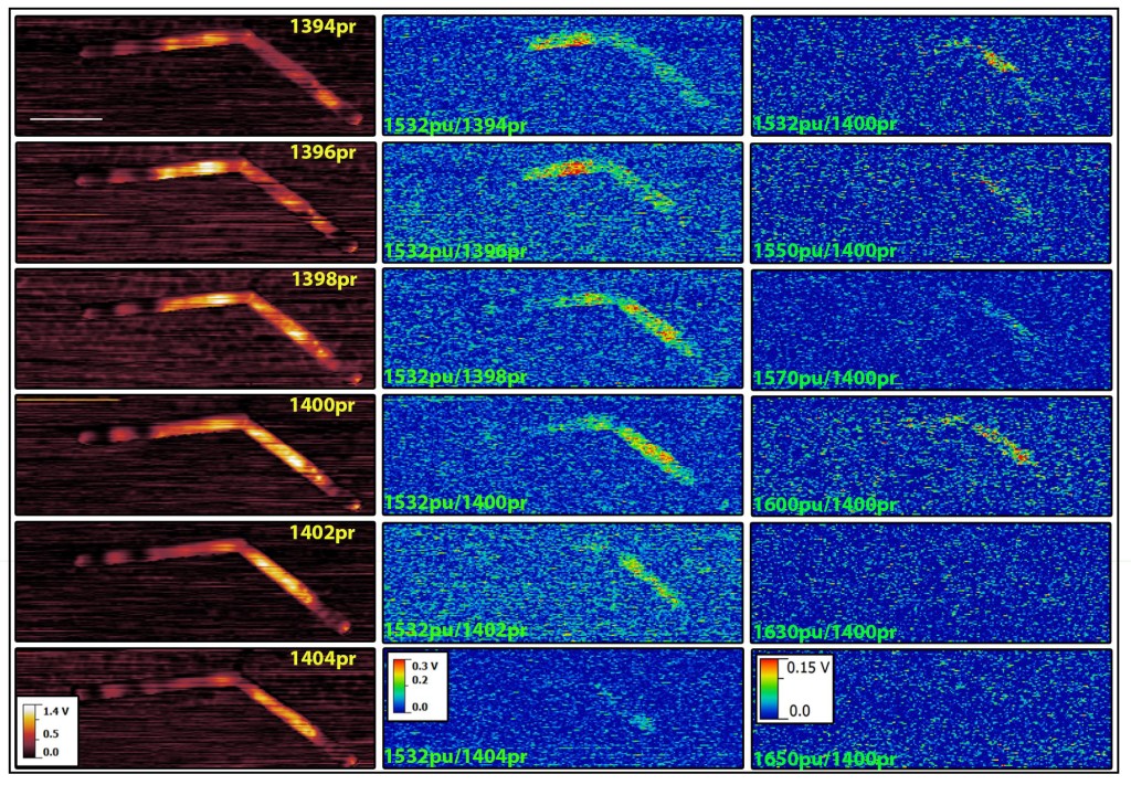
Near-field probe-only (left column) and corresponding pump-induced probe images (center column). Pump-induced probe images (right column), employing a 1400 cm–1 probing field while changing the pumping field from 1532 to 1650 cm–1. The scale bar corresponds to 500 nm.

Schematic depiction of pump-probe infrared spectroscopy on the nanoscale, based on the scattering-type scanning near-field optical microscopy approach and combined with two continuous-wave quantum cascade lasers.
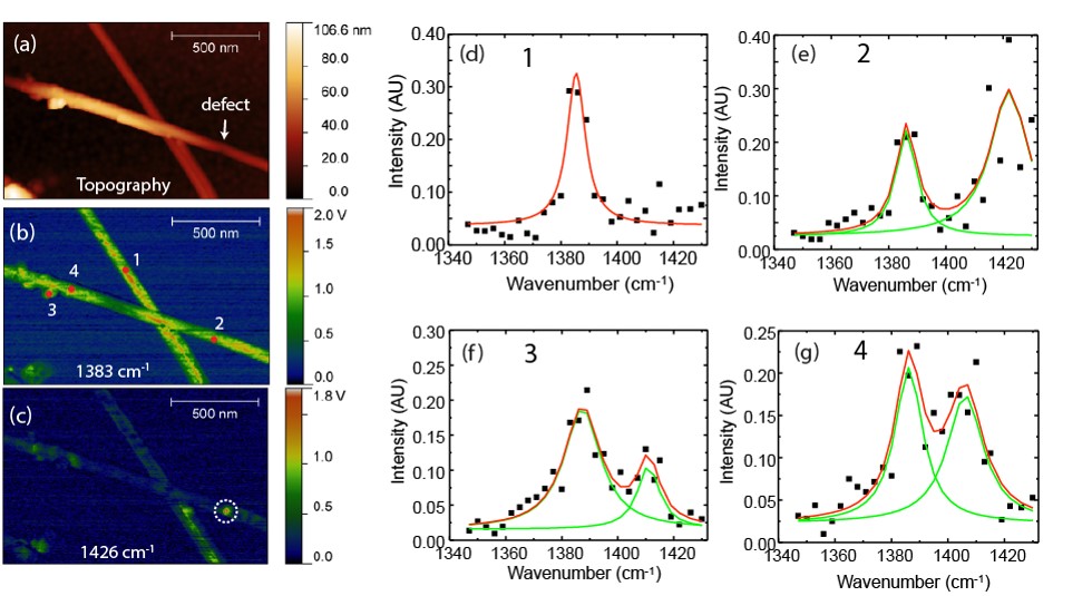
Infrared spectroscopy with 10-nm spatial resolution enables detection of structural defects in boron nitride nanotubes. (a) Topography of two crossing nanotubes. (b) Near-field image at 1383 cm–1. (c) Near-field image at 1426 cm–1. (d–g) Reconstructed near-field spectra from four individual points indicated on (b).
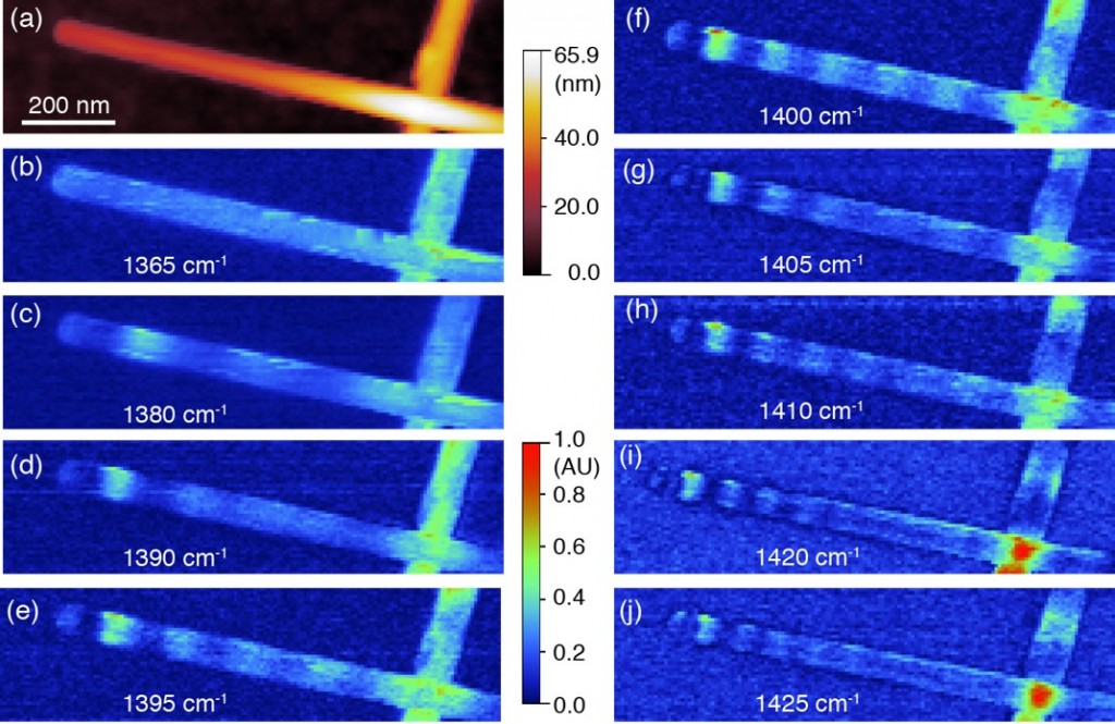
One-dimensional surface phonon polaritons in boron nitride nanotubes revealed by high-resolution infrared near-field microscopy. (a) Topography of a boron nitride nanotube. (b–j) Near-field images of the nanotube taken at wavenumbers from 1365 to 1425 cm–1.
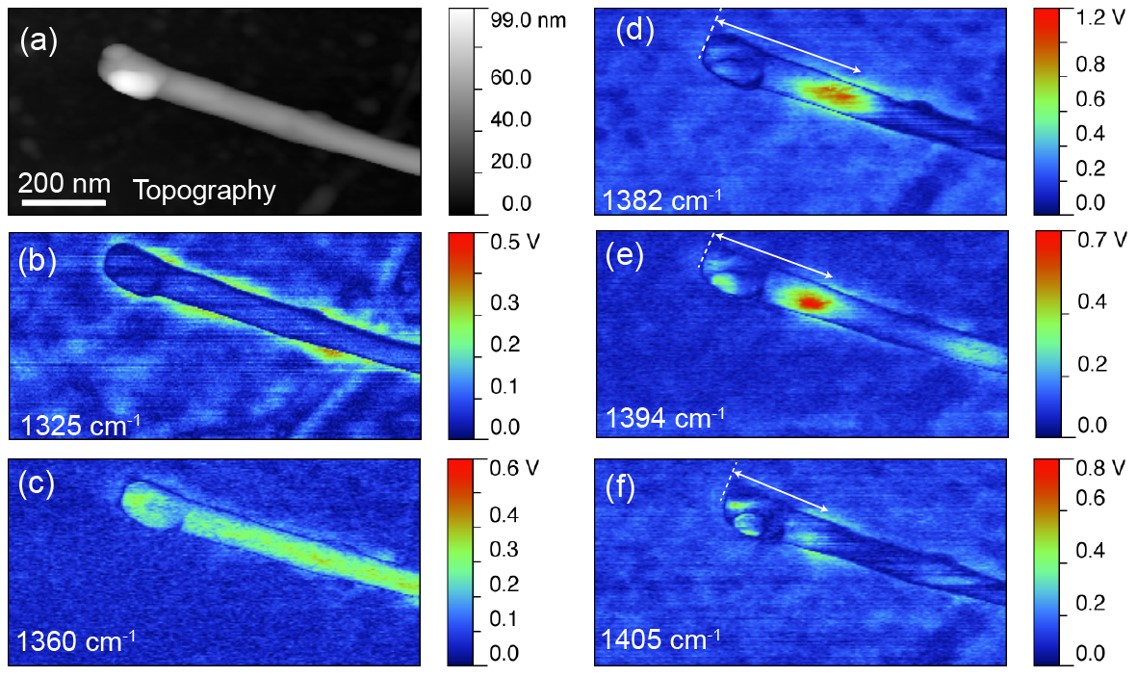
Polaritonic coupling between boron nitride nanotubes and graphene at mid-infrared frequencies. (a) Topography of a boron nitride nanotube. (b–f) Near-field images of the nanotube taken at wavenumbers from 1325 to 1405 cm–1.

Boron nitride nanotube (BNNT) near-field images at different infrared frequencies. (a) Topography of a BNNT. (b) AFM phase image of the BNNT. (c–g) Near-field images of the BNNT at 1380, 1398, 1410, 1422, and 1435 cm−1, respectively, taken with π/2 homodyne technique. (h) Fourier transformation of the SPhPs of the BNNT, showing a splitting of spatial frequency peaks. (i) Scheme of back reflections of SPhPs by nanotube terminal and gold nano-grains.
Representative publications
Ho, K.; Wei, M.; Sargent, E. H.; Walker, G. C. Grain Transformation and Degradation Mechanism of Formamidinium and Cesium Lead Iodide Perovskite under Humidity and Light. ACS Energy Lett. 2021, 6, 934–940. doi: 10.1021/acsenergylett.0c02247.
Wagner, M.; Jakob, D. S.; Horne, S.; Mittel, H.; Osechinskiy, S.; Phillips, C.; Walker, G. C.; Su, C.; Xu, X. G. Ultrabroadband Nanospectroscopy with a Laser-Driven Plasma Source. ACS Photonics 2018, 5, 1467–1475. doi: 10.1021/acsphotonics.7b01484.
Jiang, J.-H.; Xu, X. G.; Gilburd, L.; Walker, G. C. Optical hot-spots in boron-nitride nanotubes at mid infrared frequencies: one-dimensional localization due to random-scattering. Opt. Express 2017, 25, 25059–25070. doi: 10.1364/OE.25.025059.
Xu, X. G.; Jiang, J.-H.; Gilburd, L.; Rensing, R. G.; Burch, K. S.; Zhi, C.; Bando, Y.; Golberg, D.; Walker, G. C. Mid-infrared Polaritonic Coupling between Boron Nitride Nanotubes and Graphene. ACS Nano 2014, 8, 11305–11312. doi: 10.1021/nn504093g.
Xu, X. G.; Ghamsari, B. G.; Jiang, J.-H.; Gilburd, L.; Andreev, G. O.; Zhi, C.; Bando, Y.; Golberg, D.; Berini, P.; Walker, G. C. One-dimensional surface phonon polaritons in boron nitride nanotubes. Nat. Commun. 2014, 5, 4782. doi: 10.1038/ncomms5782.
Patents
Xu, X.; Walker, G. C. Method to obtain absorption spectra from near-field infrared scattering using homo-dyne detection. U.S. Patent US9404855B2, August 2, 2016.